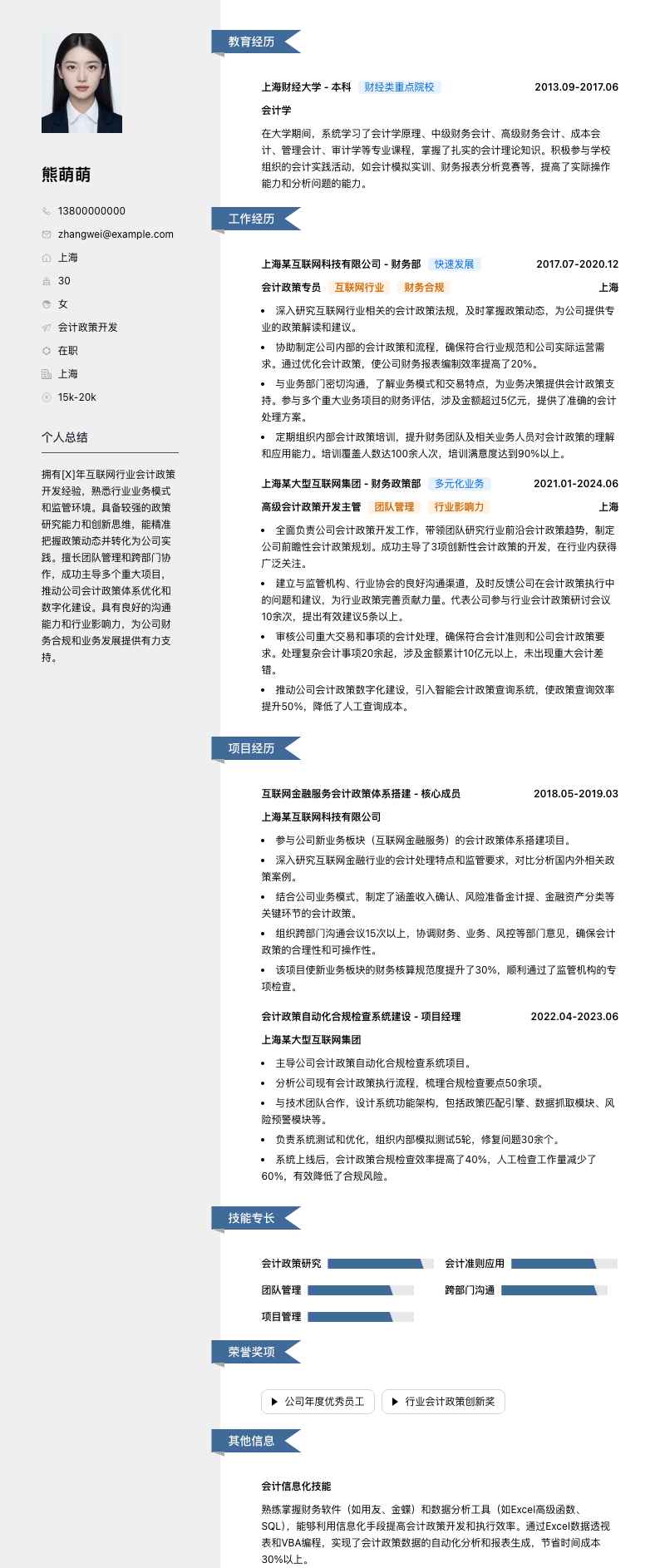
Digital IC Design Engineer简历模板


熊猫简历数字IC设计工程师简历模板,设计感、经典、左右结构风格简历模板,支持自定义板块、自定义颜色、AI润色、技能条、荣誉墙、一键更换模板,专业AI辅助一键优化数字IC设计工程师简历内容,仅需5分钟即可拥有一份精美的数字IC设计工程师简历模板,助力你获得「高薪职位」。
云端操作,实时保存
排版格式完整
打印效果最好
操作简单、制作快速,AI 智能优化
模板加载中...
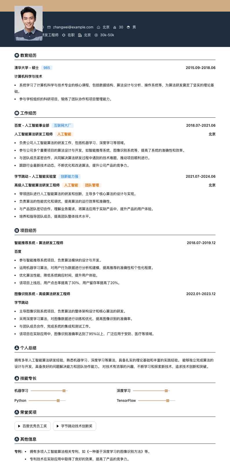
熊猫简历数字IC设计工程师简历模板,设计感、经典、左右结构风格简历模板,支持自定义板块、自定义颜色、AI润色、技能条、荣誉墙、一键更换模板,专业AI辅助一键优化数字IC设计工程师简历内容,仅需5分钟即可拥有一份精美的数字IC设计工程师简历模板,助力你获得「高薪职位」。
With [X] years of digital IC design experience, proficient in design languages such as Verilog, and well - versed in design processes such as logic synthesis and timing analysis. Possess rich project experience, successfully led and participated in the design of multiple chips, and familiar with the full process of chip from requirements analysis to tape - out and mass production. Have good teamwork ability and problem - solving ability, and can quickly respond to various challenges in design.
During college, systematically studied professional courses such as digital circuits, analog circuits, signals and systems, and mastered a solid theoretical foundation. Actively participated in practical activities such as electronic design competitions, exercising hands - on ability and teamwork ability.
Familiar with various low - power design methods, such as clock gating, multi - voltage domains, etc., successfully applied in projects, effectively reducing chip power consumption.